

OEM SiC Coated Graphite Drives Efficiency in Semiconductor Manufacturing
2026-10-14
Most process engineers don’t think of graphite carriers as a yield lever—until a contamination spike or uneven wafer heating forces a rethink. That’s where Semicorex OEM SiC coated graphite changes the picture. Its dense silicon carbide layer seals the graphite surface, cutting particle release and smoothing out thermal profiles in high-temperature steps like epitaxy and ion implantation. The result is faster cycle time, fewer defects, and consumables that last longer. Here’s how that efficiency plays out on the fab floor.
What SiC Coatings Actually Change in Graphite Performance
Most graphite users assume a SiC coating simply seals the surface against oxidation, but the real story is more layered. Once silicon carbide bonds to graphite, it closes off the open porosity that normally lets oxygen reach deep into the substrate. At high temperatures the coating forms a thin silica glass that flows into microcracks, which stops oxygen ingress far better than bare graphite ever could. What this means in practice is that coated parts survive in air at temperatures where uncoated graphite would erode within hours.
Beyond oxidation, the coating changes how graphite feels and behaves under load. SiC is much harder than graphite, so the surface goes from a soft, self-lubricating layer to a wear-resistant ceramic face. Friction against metals drops in dry conditions, but the coating also adds stiffness and creates residual stress because SiC and graphite expand at different rates. That stress can cause microcracking if the part is thermally cycled too fast, which is why coated graphite often needs more careful heating and cooling profiles than raw graphite.
Electrical and thermal behavior also shifts. The SiC layer is more electrically resistive than graphite, so surface contact resistance increases slightly, though the bulk conductivity of the part barely changes. Thermal emissivity rises, meaning coated graphite radiates heat more efficiently in vacuum furnaces. In molten metal or semiconductor processes, the coating acts as a barrier that prevents carbon from dissolving into the melt, which changes contamination levels and can extend the life of crucibles and susceptors.
Why Generic Graphite Falls Short in High-Temperature Semiconductor Processes
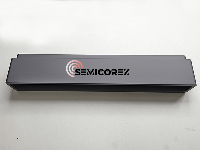
Graphite's reputation as a workhorse in thermal applications often leads engineers to assume any grade will survive the brutal conditions inside semiconductor furnaces. That assumption cracks under the reality of high-temperature processes exceeding 1,200°C, where generic graphite begins to shed particles, oxidize at the edges, and distort under thermal cycling. The problem isn't graphite itself—it's the loose, poorly controlled microstructure of off-the-shelf material. Voids between grains act as stress concentrators, and impurities like sulfur or metal traces leach out, poisoning wafers and degrading chamber atmospheres.
What separates a reliable graphite component from a failure waiting to happen is the degree of purification and densification. Generic grades often carry ash contents above 500 ppm, which is catastrophic when you're depositing films measured in angstroms. During rapid thermal processing or epitaxial growth, these contaminants migrate to the surface, creating localized hot spots or even micro-arcing. Additionally, generic graphite's coarse grain structure expands unevenly along different crystallographic axes. After a few hundred thermal cycles, that anisotropy shows up as warped susceptors, cracked wafer carriers, and process drift that no amount of calibration can fully mask.
Engineers who've chased yield losses back to their graphite fixtures quickly learn that specification sheets listing only density and flexural strength are misleading. They don't capture what happens at the atomic level when a graphite part sits at 1,400°C in a hydrogen or ammonia atmosphere—hydrogen reacts with residual oxides, creating volatile species that etch the surface, while ammonia accelerates nitrogen penetration that embrittles the bulk. Without isotropic microstructure, ultra-low impurity levels, and a pore structure engineered for specific gas chemistries, even high-purity-looking generic graphite will underperform. The real cost shows up not in the raw material invoice, but in preventative maintenance shutdowns, shortened heater lifetimes, and subtle film non-uniformities that only become obvious after thousands of wafers have been processed.
Custom OEM SiC Layers for Susceptors, Crucibles, and Liners
We work directly with equipment engineers to match the exact dimensions and surface finish required for each susceptor, crucible, or liner. Instead of forcing a stock coating onto your hardware, we adjust the SiC layer thickness, porosity, and grain structure based on the thermal cycling and chemical exposure your process actually sees.
That kind of tailoring matters most in high-temperature CVD and etch applications, where a poorly bonded layer can spall or contaminate wafers. Our coating process uses controlled CVD deposition to build a dense, adherent SiC film that handles repeated ramp-ups and aggressive cleaning chemistries without cracking.
For replacement parts and new tooling alike, you get the same lot-to-lot consistency and a documented recipe that can be reordered without lengthy requalification.
Particle Shedding and Thermal Shock Resistance in Coated Graphite
In coated graphite components, particle shedding often begins at the interface where the coating meets the substrate, especially under cyclic thermal loads. Microcracks form when expansion rates between the coating and graphite diverge, gradually loosening fine particles from the surface. These detached fragments can contaminate downstream processes or weaken the protective layer, making control of interfacial adhesion a practical priority for long-term use.
Thermal shock resistance in these materials depends less on bulk strength than on how well the coating accommodates rapid temperature swings. A thin, well-bonded layer with a graded composition tends to survive quenching better than a thick, uniform one. Tests that alternate between high-temperature exposure and rapid cooling reveal that failures often originate from edge regions or areas with residual machining stress, rather than the center of the plate.
Improving both particle retention and shock tolerance usually involves adjusting the coating's porosity and choosing a binder that does not become brittle at operating temperatures. Surface treatments that promote chemical bonding, rather than simple mechanical interlocking, reduce loose debris over repeated cycles. These refinements matter in applications like semiconductor processing or molten metal handling, where tiny shed particles or sudden coating spallation can lead to costly contamination or part replacement.
How One Fab Reduced Defect Density with SiC Coated Graphite
At one 200 mm wafer fab, the move to SiC-coated graphite started with a nagging particle problem in the epi bay. Bare graphite susceptors were wearing quickly under repeated thermal cycling, and every wet clean left a fine carbon dust in the load lock. After swapping to a CVD SiC coating on the same graphite core, the team measured a drop in added surface defects from an average of 12 per wafer down to 3 within the first month.
The coating changes how the part fails. Instead of shedding graphite flakes at the edges where gas flow is highest, the dense SiC layer holds together even after hundreds of runs. It also prevents reactive chlorine and hydrogen species from converting the underlying carbon into volatile byproducts. This mattered most in the high-temperature nitride and oxide steps, where previous defects clustered near the wafer flat.
Qualification wasn't just a drop-in. The fab checked coating thickness uniformity, edge coverage, and post-coat outgassing before committing the full tool set. Maintenance intervals doubled, and the defect excursions tied to susceptor replacement disappeared. By the end of the quarter, the lower defect density translated into about two extra yielding wafers per lot.
The Hidden Cost of Uncoated Graphite in Semiconductor Manufacturing
Uncoated graphite components quietly erode process stability in wafer fabrication. Without a protective layer, the material sheds micro-particles during thermal cycling, contaminating chambers and driving up defect densities. These subtle losses rarely trigger immediate alarms, yet they accumulate as yield drag and unplanned tool downtime.
The financial impact hides in plain sight: more frequent preventive maintenance, shorter consumable lifetimes, and the need for additional wafer inspections to catch sporadic particle fallout. Engineers often compensate by increasing purge cycles or lowering throughput, which effectively taxes the entire production line instead of addressing the root material weakness.
Over a quarter of operation, the absence of a coating translates into higher cost per wafer than the initial savings on cheaper graphite blanks. By the time the correlation between particle excursions and uncoated surfaces becomes clear, the accumulated margin erosion has already outpaced any upfront discount.
FAQ
The coating creates a chemically inert surface that resists oxidation and thermal shock, so susceptors and carriers maintain flatness across hundreds of heating cycles. That flatness keeps temperature gradients low enough to prevent slip lines and dopant drift on 300mm wafers.
Bare graphite sheds particles as it oxidizes at process temperatures. SiC seals the porous graphite structure, cutting particle release by roughly an order of magnitude, and its hardness protects against erosion from aggressive cleaning gases like ClF3 or NF3.
The dense CVD or sintered SiC layer prevents microcracks from opening under thermal cycling. It also has a low coefficient of friction against silicon wafers, so backside scratching and graphite dust generation drop sharply during load/unload steps.
You'll find it in epitaxial growth susceptors, ion implantation beam stops, plasma etch chamber liners, and wafer carriers for LPCVD and RTP. Each application uses the same base benefit: dimensional stability under extreme heat plus resistance to reactive species.
SiC has a thermal conductivity around 120 W/mK, close to graphite's own, so it doesn't act as an insulating blanket. Its flexural strength above 400 MPa prevents sagging at 1600°C, while its low CTE mismatch with graphite minimizes delamination.
Thin coatings below 100 microns preserve most of graphite's high in-plane thermal conductivity and are cheaper, but they wear faster in plasma environments. Thicker coatings of 200–300 microns extend service life to over two years in aggressive etchers but slightly reduce heat transfer uniformity.
Avoid rapid cooling from process temperature to room temperature with forced air; ramp down at less than 10°C per minute. Inspect coating edges under 20x magnification for hairline cracks, and use isopropyl alcohol wipes instead of abrasive scrubbers to remove residues.
Yes, if the graphite substrate hasn't oxidized through more than 0.5mm of thickness. Reputable OEMs grind away the damaged SiC layer, re-coat by CVD, and re-machine critical tolerances, typically restoring 80–90% of original lifespan at about half the cost of new parts.
Conclusion
In semiconductor manufacturing, graphite components like susceptors, crucibles, and liners sit at the center of high-temperature processes. Bare graphite brings inherent risks: porous surfaces trap contaminants, edges shed particles under thermal cycling, and repeated exposure to aggressive process gases accelerates erosion. Applying an OEM silicon carbide coating changes these failure modes. The dense, chemically inert SiC layer seals the graphite substrate, blocking outgassing and preventing unwanted dopant migration. It also tunes surface emissivity and electrical properties to match specific process recipes. Unlike off-the-shelf coated parts, custom OEM SiC layers are engineered for the part's geometry and thermal load, creating a uniform barrier that withstands rapid heating and cooling without cracking or delamination. That matters because generic graphite falls short where wafer-level uniformity demands tight control over temperature and contamination.
A real-world example illustrates the payoff. One fab replaced uncoated graphite fixtures with OEM SiC coated components and recorded a measurable drop in defect density, traced directly to reduced particle shedding and fewer micro-cracks after thermal shock. The hidden costs of uncoated graphite go beyond replacement frequency: every particle release can trigger rework, tool downtime, and yield loss that quietly erodes margins. Coated graphite also survives longer between maintenance cycles because the SiC layer resists oxidation and chemical attack in fluorine and chlorine environments. For high-mix fabs, tailoring the coating thickness, porosity, and surface finish to each carrier or liner means fewer process excursions and more stable deposition rates. Ultimately, investing in OEM SiC coated graphite is less about the material itself and more about removing variability from semiconductor manufacturing, where consistent thermal performance and particle control directly drive wafer throughput and profitability.
Contact Us
Contact Person: Svenja Wei
Email: [email protected]
Tel/WhatsApp: +8613567891907
Website: https://www.semicorex.com